Light and Electromagnetic Waves in Research for New Technologies
Apr 30th 2022
Magnetic property in an antiferromagnetic semiconductor enables light manipulation on the nanoscale
by Melissa Pappas, University of Pennsylvania (April 11, 2022)
A major research challenge in the field of nanotechnology is finding efficient ways to control light, an ability essential for high-resolution imaging, biosensors and cell phones. Because light is an electromagnetic wave that carries no charge itself, it is difficult to manipulate with voltage or an external magnetic field. To solve this challenge, engineers have found indirect ways to manipulate light using properties of the materials from which light reflects. However, the challenge becomes even more difficult on the nanoscale, as materials behave differently in atomically thin states.
Deep Jariwala, Assistant Professor in Electrical and Systems Engineering, and colleagues have discovered a magnetic property in antiferromagnetic materials that allows for the manipulation of light on the nanoscale, and simultaneously links the semiconductor material to magnetism, a gap that scientists have been trying to bridge for decades. They described their findings in a recent study published in Nature Photonics.
Collaborating with Liang Wu, Assistant Professor in the Department of Physics and Astronomy in Penn's School of Arts and Sciences, along with graduate students Huiqin Zhang, a doctoral student in Jariwala's lab, and Zhuoliang Ni, a doctoral student in Wu's lab, the researchers describe the magnetic property of FePS3, an antiferromagnetic semiconductor material. Christopher Stevens and Joshua Hendrickson of the Air Force Research Laboratory and KBR, Inc. in Ohio, as well as Aofeng Bai and Frank Peiris at Kenyon College in Ohio also contributed to this work.
"Our lab's research focuses on finding new materials for electronics, computers, information storage and energy harvesting and conversion," says Jariwala. "The class of materials we examine are atomically thin two-dimensional van der Waals materials, and more specifically, those that are semiconducting."

Magnetic materials are classified as either ferromagnets or antiferromagnets. Antiferromagnets are materials that contain lines of electrons spinning in one direction next to lines of electrons spinning the opposite direction, canceling out any attraction or repulsion forces typical of magnets, whereas ferromagnets are those with electrons that all spin in the same direction and produce their own magnetic field.
The antiferromagnetic material used in this study, FePS3, or iron phosphorus trisulfide, is a semiconductor with unique optical properties dependent on the alignment of its electron spin direction.
"Theoretically, by applying an external magnetic field to this antiferromagnetic 2D semiconductor, we can alter its optical properties," says Jariwala. "And that is how you use a magnetic property to manipulate light. Having made the link between magnetism and light manipulation, we are entering into the field of 'magnetophotonics,' an area of research I believe will greatly expand in the next five to ten years."
The paper not only describes the use of the material's magnetic properties to control light, it highlights that there is also a physical property of the material involved as well.
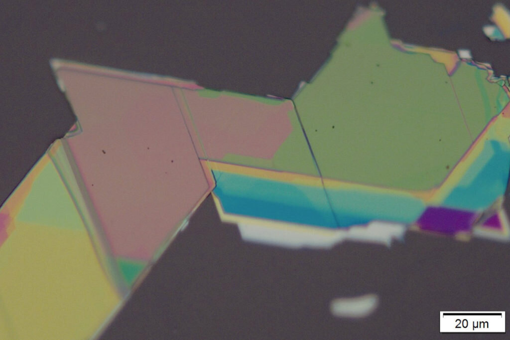
"We also find that for specific thicknesses this antiferromagnetic material acts as a cavity that significantly enhances its interaction with light and its alteration with the magnetic property," says Jariwala. "This is important when trying to develop an efficient technique for light control."
"Imagine the cavity of the material as the space between two parallel mirrors," he says. "Standing in this space, you will see an infinite number of your own reflections, which occurs because the light you are observing is interacting with the medium of the mirrors many times. The more interactions the light has with the medium before it escapes, the stronger the optical effect. By creating a highly interactive cavity through changing the thickness of the material, we can produce strong optical responses, only now they are also guided by the magnetic property of the semiconductor."
Jariwala's work links the magnetic and optical properties of antiferromagnetic nanomaterials, opening doors for engineering light for high-tech applications.
The manipulation of light is not only significant for technology advancement, it is also a tool used to characterize materials.
"This work also relates to a previous study led by Liang that demonstrated the ability of second harmonic generation microscopy to directly image the spin alignment in a different antiferromagnetic semiconductor at the monolayer level," says Jariwala.
"This type of microscopy is a specialized way to observe a unique optical property only present in certain materials. Using this specialized microscopy technique, we can now characterize materials and map their magnetic properties with a thickness of just a few atoms. These papers together highlight the significance of optical properties in both understanding materials better and developing new kinds of imaging and microscopy techniques." says Wu
The researchers' next steps will be to bring the theory of light manipulation by magnetism to practice by actively applying magnetic fields to selected orient spins in antiferromagnetic materials, testing the ability to create magnetophotonic circuits.
"We are very excited by these observations, particularly because they are in semiconductor materials where we possess various other knobs for manipulation," says Jariwala. "In addition, this class of materials is much broader with many more combinations to explore, including finding ways to raise the magnetic transition temperatures. We are now looking to find and design ways to manipulate light inside these materials using multiple control knobs and see how strongly we can tune them in real devices."
Photo: The different colors in this sample of iron phosphorous trisulfide (FePS3) correspond to regions with varying thicknesses, which form different “cavity” modes at different wavelengths. Credit: University of Pennsylvania

